
Modern electronic devices would be much different than they are today if it were not for the printed circuit board (PCB). It can be easy to overlook the significance of PCBs and instead focus on the latest and greatest chips mounted on them, but if not for the PCB, we would not have electronic devices that are so compact and inexpensive, or circuits that are so reliable and consistently manufactured. These boards are often very complex, so naturally errors can be introduced at any stage, from design to production. And an error can have serious consequences, from frying all the chips on it to starting a fire, and of course the cost of shipping a flawed product can be massive in terms of both dollars and damaged reputation.
To prevent problems from slipping through quality control departments, automated inspection systems have been developed. These generally work pretty well, but as designs grow ever more complex while shrinking to smaller and smaller sizes, it becomes more difficult to detect every problem. Engineer Solomon Githu recently came up with an idea that tackles PCB defect recognition in an unconventional manner. The core of the idea is to use computer vision and machine learning to rapidly pick out any potential errors that could result in faulty circuits. Considering the challenges surrounding this problem, any additional safeguards that can be put in place would be welcome.
Githu wanted to use an object detection algorithm so that the exact type, and location, of each defect could be found and reported. Designing an accurate object detection model can be quite a chore, so the Edge Impulse machine learning platform was used to simplify and streamline the process. But before getting started with the algorithm design, sample data would be needed to help the model learn. A subset of Kaggle’s PCB Defects dataset was chosen, with three different types of defects (missing hole, open circuit, and short circuit) being included for this proof of concept.
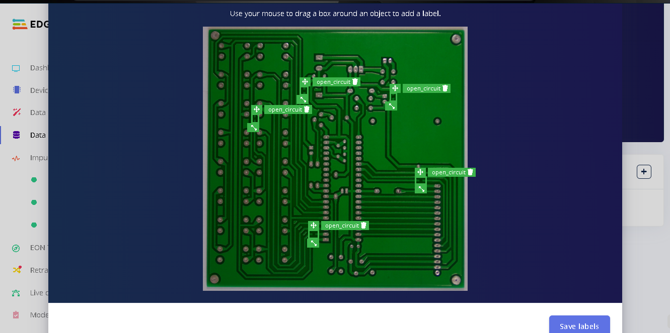
A total of 887 images for training and 253 images for testing were uploaded to Edge Impulse. The labeling queue tool was then used to draw bounding boxes around each type of defect, so that the model could be trained to recognize what they look like. That is quite a few images to label, but fortunately the labeling queue tool has an AI-assisted labeling feature that positions the bounding boxes for you — it is only necessary to make occasional, small adjustments to fine-tune the suggestions.
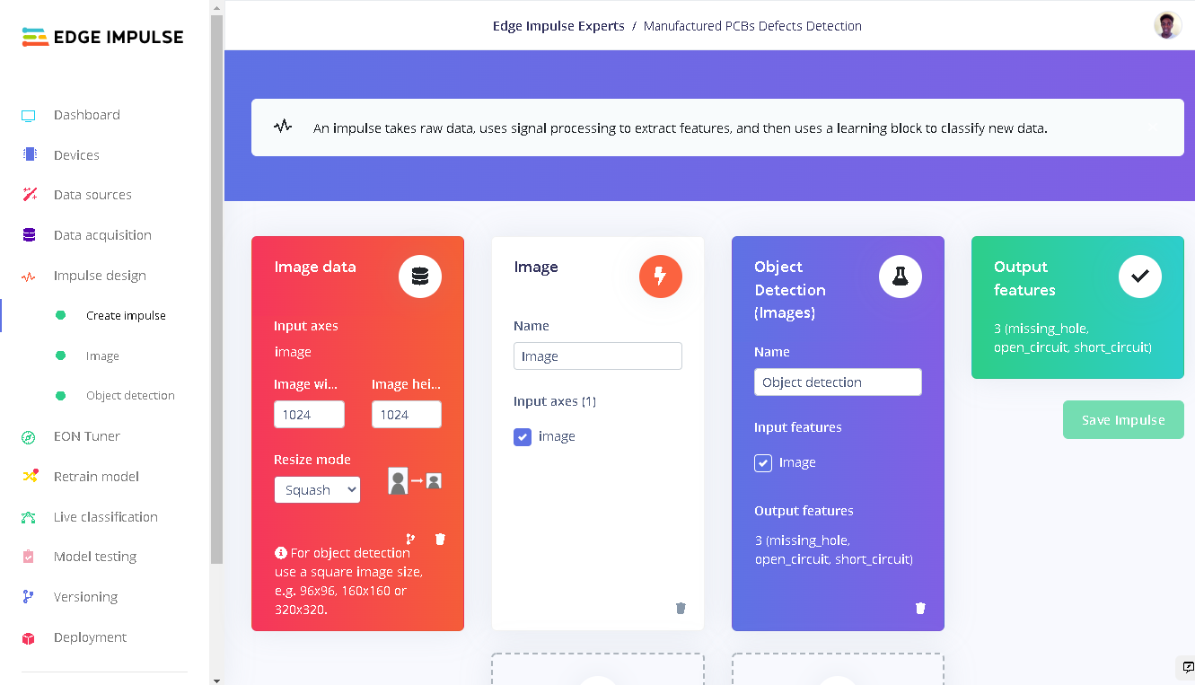
With the data wrangling out of the way, Githu started building the impulse that would perform the PCB defect detections. During design, multiple model types were experimented with. First a YOLOv5 model was tested, but the performance was very poor — this was most likely because YOLOv5 struggles to detect small objects that appear in groups, which is exactly the type of data one finds in PCB images. It is also recommended that YOLOv5 models be trained with more than 1,500 images per class, which is more data than Githu could come by. Next, Edge Impulse’s FOMO object detection algorithm was tested. Since it does not suffer from the aforementioned issues with YOLOv5, the results proved to be much better. With the model testing results looking good, the defect detection algorithm was good to go.
For this device to provide real time PCB defect checks, the model would need to be deployed to an edge computing device. A Raspberry Pi 4, which provides more than enough compute power for the lightweight FOMO algorithm, was selected. The addition of an 8-megapixel Raspberry Pi Camera was all that was needed to complete the hardware design. After installing the Edge Impulse CLI, the entire object detection pipeline could be deployed to the Raspberry Pi with a single command.
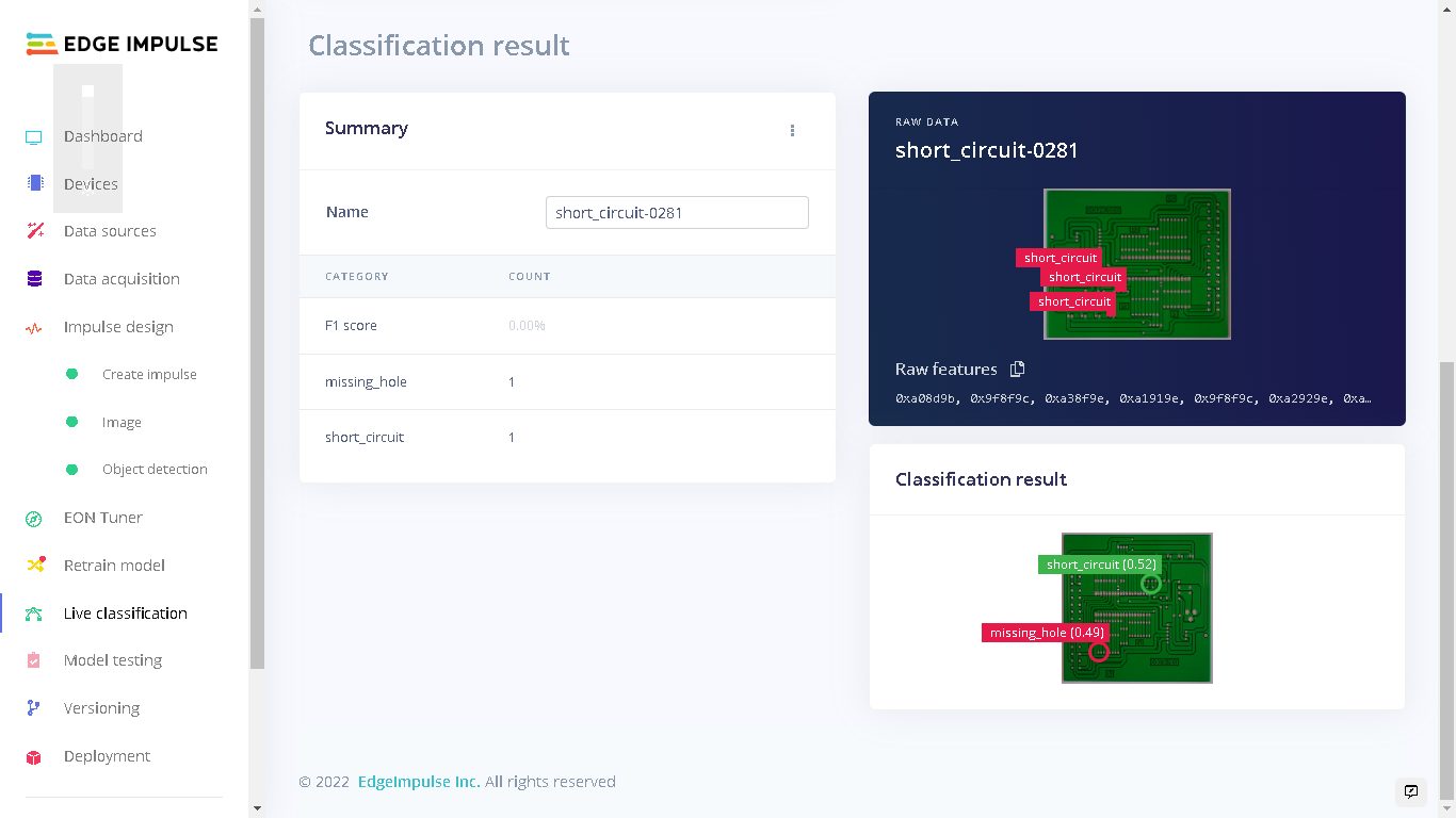
Once the deploying was deployed, a live classification tool was automatically made available as a local web application running on the Raspberry Pi. After kicking the tires for a bit, Githu found that the PCB defect detector was doing the job it was created for — successfully locating problems with PCBs. While the model ran more than fast enough for a proof of concept, Githu notes that higher speed detections may be needed in commercial settings, and the hardware may need to be upgraded to something like an NVIDIA Jetson. Since Edge Impulse supports the Jetson (and many other platforms), deploying the model to one would just take a few clicks in Edge Impulse Studio.
Githu’s work has shown that machine learning may be a viable option for performing additional quality control checks on PCBs. He hopes to extend his work in the future by exploring how multi-layer PCBs could be inspected using similar methods. If you have some ideas about how this project could be made even better, feel free to clone Githu’s public Edge Impulse project and show us what you can do! Be sure to read up on the documentation first to give yourself a head start.
Want to see Edge Impulse in action? Schedule a demo today.